Expertise
Custom electronic board design
Schematic capture, multilayer PCB layout, firmware and DFM — our engineers design your board from A to Z, entirely in-house, with production-ready deliverables.
300+ boards designed,
all in-house
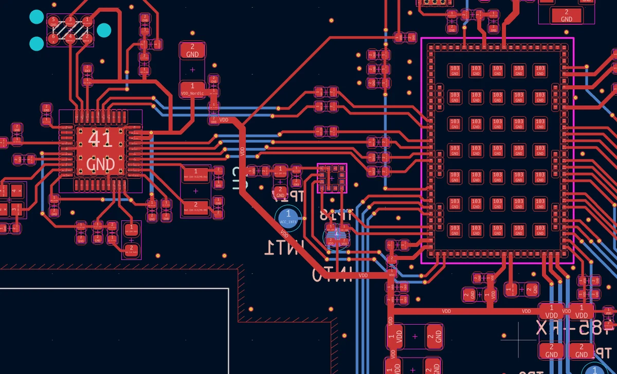
Custom electronic board design has been our core business since Codium was founded. Schematic capture, component footprints, multilayer PCB layout, DRC/ERC verification — every step is carried out by our own engineers, with no subcontracting.
We work on boards of every level of complexity: from a simple 2-layer module to high-density 8-layer boards with controlled-impedance constraints, RF or high-speed design.
Our deliverables go to manufacturing in under a week: Gerber files, BOM, complete manufacturing package. Directly usable by any PCB manufacturer.
What we
can design
Our engineers cover every family of electronic design.
STM32, NRF52, ESP32, i.MX, Raspberry Pi Compute Module. SPI, I²C, UART, USB and Ethernet interfaces. Design of power planes and decoupling.
Routing of RF lines with impedance constraints, coaxial transitions, shielding vias. PCB antenna design (patch, PIFA, dipole). In-house pre-qualification.
DDR, USB 3, PCIe, LVDS, Gigabit Ethernet — differential length constraints, terminations, via stubs. Signal integrity simulation when needed.
Acquisition chains, operational amplifiers, high-resolution ADCs/DACs, current sensors, precision measurement. Separation of digital/analogue planes.
DC/DC converters, Li-Ion/LiPo battery management, chargers, protection. Thermal sizing, power traces, copper pours.
4- to 8-layer stackups, BGA, QFN, LGA. Via-in-pad, microvias where required. Continuous DFM to guarantee manufacturability in volume.

From spec
to validated Gerber
Our design process is structured to deliver boards that work first time and are ready for volume production without modification.
Selection of key components, system architecture, power and EMC constraints. Feasibility validation before starting the schematic.
Complete electronic schematic with ERC verification. Verified component libraries. Internal review before moving on to layout.
Placement, routing, plane management, impedance constraints. Final DRC before export. Stackup template optimised for the target manufacturer.
Gerber, BOM and complete manufacturing package delivered in under a week. Prototype built on our production line or by an external manufacturer as required.
Designed to be manufactured — not just to work
A board that works as a prototype but cannot be produced in volume is a costly failure. At Codium, the design office and production sit within the same company — our engineers design with real manufacturing constraints in mind.
Continuous DFM: trace width and spacing matched to the manufacturing equipment, footprints verified for automated placement, BOM organised to limit the number of part references. The result: fewer surprises at industrialisation and shorter time to volume production.
Our production line →
Frequently asked questions — PCB design
The most common technical questions about our design process.
How many layers can Codium handle for a PCB?
Codium designs PCBs from 2 to 8 layers (and more on request). 4-layer boards are the standard for designs with EMC constraints or high density. 6- and 8-layer boards are used for high-speed, RF or very high component density designs.
What files do you deliver at the end of the design?
Standard deliverables include: Gerber files (copper layers, solder mask, silkscreen, outline), Excellon drill file, BOM (bill of materials) with part references and suppliers, and a complete manufacturing package with assembly notes and component centroids for automated placement.
All deliverables are DRC/ERC-checked before delivery.
Do you work on RF or high-frequency designs?
Yes. Codium has an in-house RF specialist with the measurement equipment to tune antennas and pre-qualify RF front-ends. We handle controlled-impedance constraints, coaxial transitions, microstrip lines and shielding vias.
Can you design from an existing schematic?
Yes. If you already have an electronic schematic (in KiCad, Altium, Eagle or another tool), Codium can take on the PCB layout only, or take over the whole design to improve it and prepare it for production.
What is DFM and why does it matter?
DFM (Design for Manufacturing) is the set of design rules that ensure a board can be manufactured reliably in volume. At Codium, the design office and production sit within the same company: our engineers design with real manufacturing constraints in mind — which avoids costly surprises at industrialisation.
Need custom PCB design?
Share your project in an initial conversation — we will tell you what we can do, how long it will take and what it will cost.