Electronic schematic
Complete design : power supply, microcontrollers, IoT connectivity, display interfaces, sensors. Timing, power and signal integrity constraints managed from the schematic stage.
Design Office
From component to production-ready board — schematic, layout, DFM, all in-house
At Codium, schematic design and PCB layout are not subcontracted. The person who drew the schematic routes the board — they know every constraint by heart. The result : fewer back-and-forths, greater responsiveness, a board designed for production from the very first trace.
This continuity between schematic and layout eliminates the loss of information usually caused by handing over between two design offices or two engineers. DFM optimisations are built in from the schematic phase, not discovered at layout time.
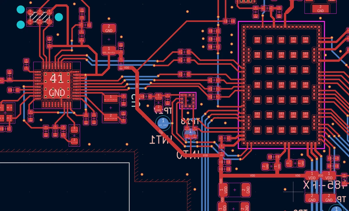
Every PCB design discipline is mastered in-house — from schematic timing constraints through to the final export.
Complete design : power supply, microcontrollers, IoT connectivity, display interfaces, sensors. Timing, power and signal integrity constraints managed from the schematic stage.
From 2 to 8+ layers, high density, BGA, fine-pitch QFP. Controlled-impedance constraints, differential routing, ground plane management.
USB 3, Gigabit Ethernet, DDR, MIPI, LVDS. Impedance control, length matching, careful decoupling for demanding high-speed interfaces.
Built-in test points, optimised stencil margins, footprints validated in production. The board is designed for our workshop from the start — no surprises at industrialisation.
In-house libraries debugged and validated in production. Footprints optimised from field feedback : stencil apertures, solder mask relief zones.
Complete manufacturing package : Gerber, BOM, Pick & Place, 3D view for mechanical integration. Industry-standard formats.
When schematic and layout are done by the same engineer, you gain time, quality and responsiveness. The engineer who drew the schematic knows every electrical constraint by heart — there is no need to relearn them at layout. DFM optimisations are built in from the schematic phase rather than discovered too late. Changes — frequent on any real project — are handled immediately, with no file handover and no loss of context between two people.
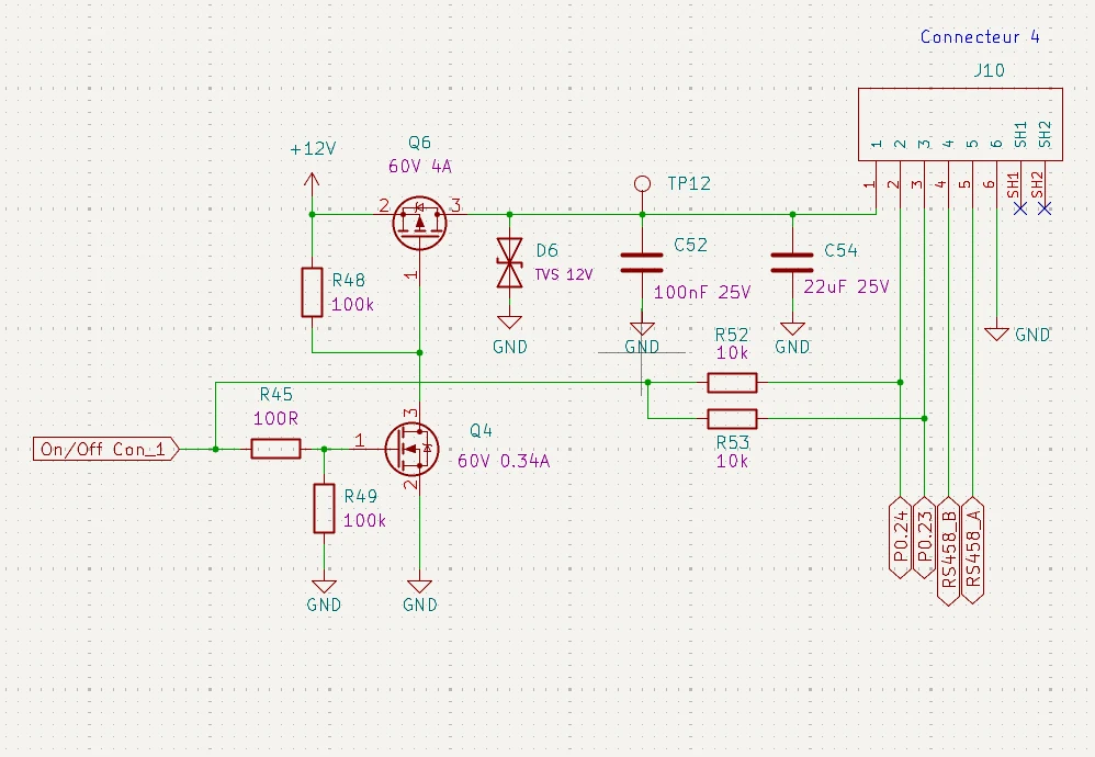

Whether you are starting from a blank sheet or already have an existing schematic to optimise, we step in at every stage of PCB design.
Once the requirements are frozen and the components chosen, a production-ready schematic + layout takes no more than a week. And because manufacturing takes place in our own workshops, the same engineer follows the industrialisation — no loss of information, no handover risks.
Codium has used KiCad since the company was founded, for all of its projects. Open source, backed by CERN, with native 3D export and compatible with industry-standard formats. Source files are handed over to the customer with no licence restrictions — no proprietary software, no long-term lock-in risk.
Our symbol and footprint libraries are maintained in-house and validated in production. Every footprint is verified on a first prototype before being permanently added to the library.
Our experience with KiCadTell us your constraints — number of layers, critical components, lead times. We will get back to you quickly with an estimate.
